Quick Charge 2.0 Powerbank Adapter Board
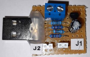
A small adapter board which emulates a Quickcharge 2.0 (also compatible with Quick Charge 3.0) capable device to force a power supply or a powerbank to output higher voltages.
Quick Charge 2.0 specification
The output Voltage can be configured by applying different voltage levels to the USB data lines D+ and D-:
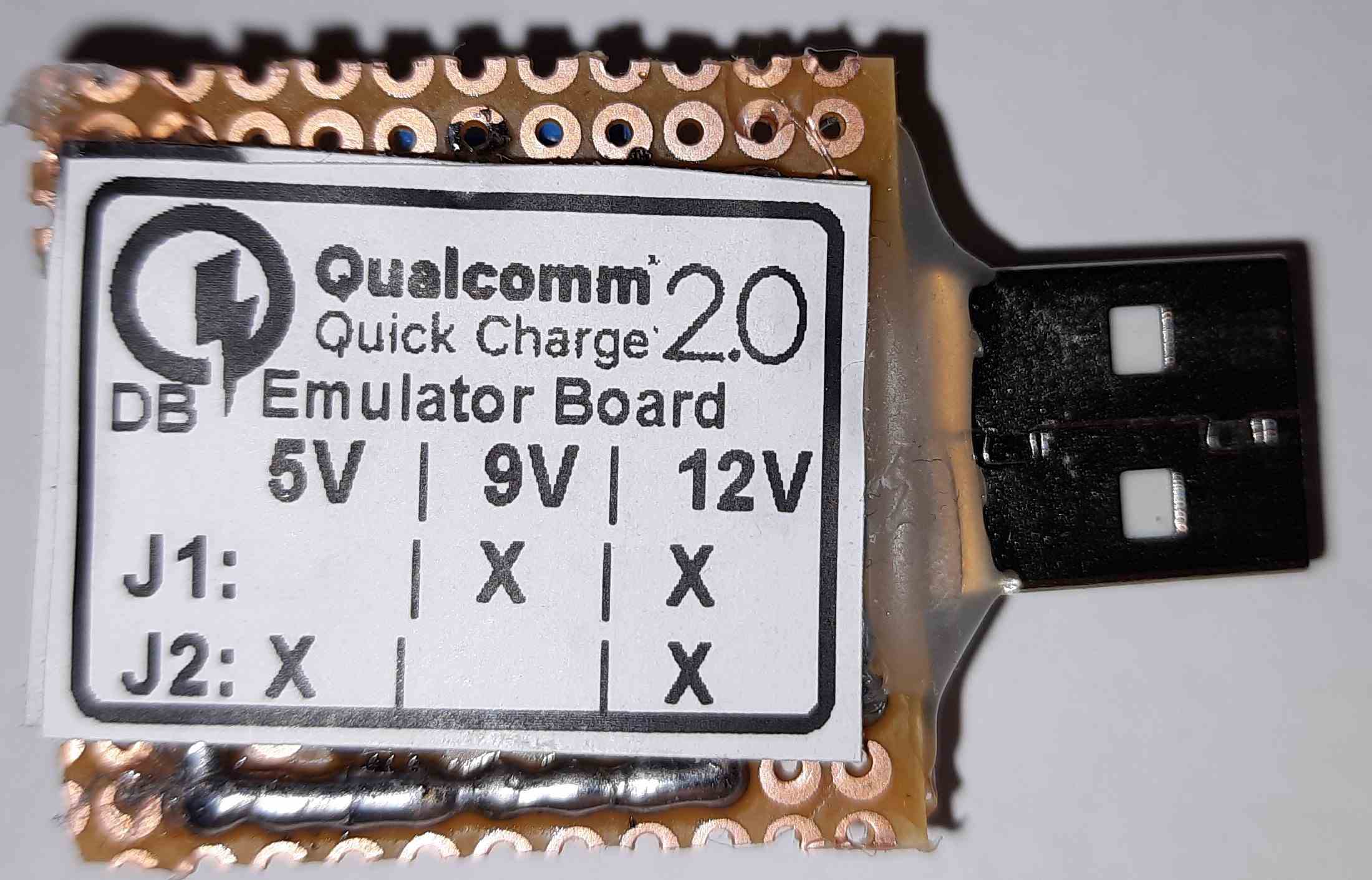
With this board these Voltage levels are set by different jumper settings.
Please note that due to the Quick Charge specification the jumper settings have to be done AFTER inserting the adapter into the power supply or powerbank. After plugging in the adapter, the powerbank will output 5V no matter how the jumpers are set. Higher voltage outputs can only be achieved by changing the jumper settings after inserting.
Voltage Levels:
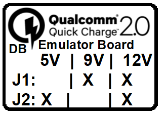
| D+ | D- | output voltage | Jumper positions: | J1 | J2 |
|---|---|---|---|---|---|
| 0,6V | 0,0V | 5V (default) | x | ||
| 3,3V | 0,6V | 9V | x | ||
| 0,6V | 0,6V | 12V | x | x |
Jumper positions: x = set, blank = not set
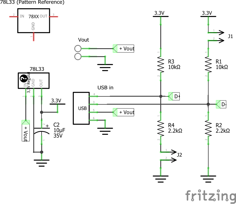
Schematic
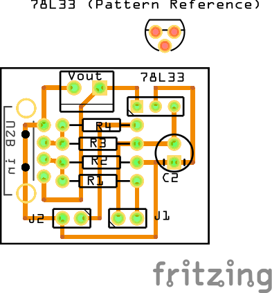
PCB Layout
You can download the fritzing file here (QC2_adapter_board.zip):
PCB Label
Sources
- https://www.mouser.com/datasheet/2/328/chiphy_family_datasheet-269468.pdf
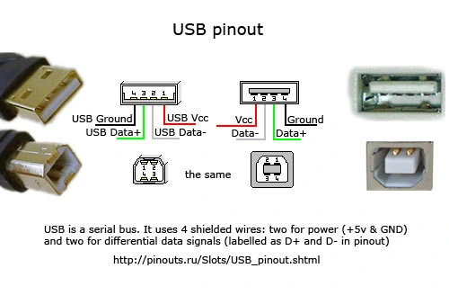
- USB pinout: https://www.electroschematics.com/wp-content/uploads/2010/01/usb-pinout.jpg
I hope you like this project!
This work by Dustin Brunner is licensed under CC BY 4.0

Dieses Werk von Dustin Brunner ist lizenziert unter einer Creative Commons Namensnennung 4.0 International Lizenz.
0 Kommentare